- 您现在的位置:买卖IC网 > Sheet目录1993 > DS1308U-3+ (Maxim Integrated Products)IC RTC 56BYTE NVRAM I2C 8UMAX
DS1308
Low-Current I2C RTC with 56-Byte NV RAM
2
Maxim Integrated
(All voltages relative to ground.)
Voltage Range on VCC or VBAT ...........................-0.3V to +6.0V
Voltage on Any Non-Power Pin................ -0.3V to (VCC + 0.3V)
Operating Temperature Range.......................... -40NC to +85NC
Junction Temperature Maximum.....................................+150NC
Storage Temperature Range............................ -55NC to +125NC
Lead Temperature (soldering, 10s) ................................+300NC
Soldering Temperature (reflow) ......................................+260NC
ABSOLUTE MAXIMUM RATINGS
Stresses beyond those listed under “Absolute Maximum Ratings” may cause permanent damage to the device. These are stress ratings only, and functional opera-
tion of the device at these or any other conditions beyond those indicated in the operational sections of the specifications is not implied. Exposure to absolute
maximum rating conditions for extended periods may affect device reliability.
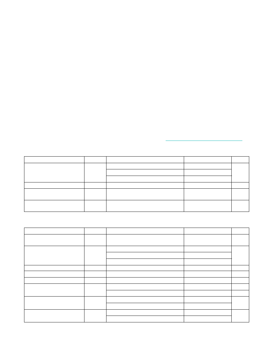
RECOMMENDED OPERATING CONDITIONS
(TA = -40NC to +85NC, unless otherwise noted.) (Note 2)
DC ELECTRICAL CHARACTERISTICS
(VCC = VCCMIN to VCCMAX, VBAT = VBATMIN to VBATMAX, TA = -40NC to +85NC, unless otherwise noted.) (Note 2)
F
SOP
Junction-to-Ambient Thermal Resistance (BJA) .....206.3NC/W
Junction-to-Case Thermal Resistance (BJC) ...............42NC/W
Note 1: Package thermal resistances were obtained using the method described in JEDEC specification JESD51-7, using a four-layer
board. For detailed information on package thermal considerations, refer to www.maximintegrated.com/thermal-tutorial.
PACKAGE THERMAL CHARACTERISTICS (Note 1)
PARAMETER
SYMBOL
CONDITIONS
MIN
TYP
MAX
UNITS
Operating Voltage Range
VCC
DS1308-18
1.71
1.8
5.5
V
DS1308-3
2.7
3.0
5.5
DS1308-33
3.0
3.3
5.5
Battery Voltage
VBAT
1.3
5.5
V
Logic 1 Input
VIH
0.7 x
VCC
VCC +
0.3
V
Logic 0 Input
VIL
-0.3
0.3 x
VCC
V
PARAMETER
SYMBOL
CONDITIONS
MIN
TYP
MAX
UNITS
Power-Supply Active Current
(Note 3)
ICCA
fSCL = 400kHz
325
F
A
Power-Supply Standby Current
(Note 4)
ICCS
-33: VCC = 3.63V
125
F
A
-18: VCC = 1.89V
100
VCC = VCCMAX
200
Battery Leakage Current
IBATLKG
VCC R VPF
-100
25
+100
nA
Input Leakage (SCL)
II
VIN = 0V to VCC
-0.1
+0.1
F
A
I/O Leakage (SDA, SQW/CLKIN)
IIO
I2C bus inactive, ECLK = 1
-0.1
+0.1
F
A
Output Logic 0 (SDA, SQW/
CLKIN), VOL = 0.4V
IOL
VCC R VCCMIN
3.0
mA
VBAT R 1.3V R VCC + 0.2V
250
F
A
Power-Fail Trip Point
VPF
-33
2.70
2.82
3.00
V
-18
1.45
1.62
1.70
Switchover Voltage
VSW
VBAT > VPF
VPF
V
VBAT < VPF
VBAT > VCC
发布紧急采购,3分钟左右您将得到回复。
相关PDF资料
DS1315EN-5/T&R
IC TIME CHIP PHANTOM 20-TSSOP
DS1318E+
IC COUNTER ELAPSED TIME 24-TSSOP
DS1337S+C01
IC RTC SERIAL 2WIRE LP 8-SOIC
DS1338C-33#T&R
IC RTC 56BYTE NV SRAM 16SOIC
DS1339AU+
IC RTC I2C W/ALARM 8USOP
DS1339C-2#
IC RTC I2C W/ALARM 16-SOIC
DS1340Z-33/T&R
IC RTC I2C W/CHARGER 3.3V 8-SOIC
DS1340Z-3
IC RTC I2C W/CHARGER 3V 8-SOIC
相关代理商/技术参数
DS1308U-3+T
功能描述:实时时钟 LOW CUR 3V I2C RTC
RoHS:否 制造商:Microchip Technology 功能:Clock, Calendar. Alarm RTC 总线接口:I2C 日期格式:DW:DM:M:Y 时间格式:HH:MM:SS RTC 存储容量:64 B 电源电压-最大:5.5 V 电源电压-最小:1.8 V 最大工作温度:+ 85 C 最小工作温度: 安装风格:Through Hole 封装 / 箱体:PDIP-8 封装:Tube
DS1308U-33
制造商:MAXIM 制造商全称:Maxim Integrated Products 功能描述:Low-Current I2C RTC with 56-Byte NV RAM
DS1308U-33+
功能描述:实时时钟 LOW CUR 3.3V I2C RTC
RoHS:否 制造商:Microchip Technology 功能:Clock, Calendar. Alarm RTC 总线接口:I2C 日期格式:DW:DM:M:Y 时间格式:HH:MM:SS RTC 存储容量:64 B 电源电压-最大:5.5 V 电源电压-最小:1.8 V 最大工作温度:+ 85 C 最小工作温度: 安装风格:Through Hole 封装 / 箱体:PDIP-8 封装:Tube
DS1308U-33+T
功能描述:实时时钟 LOW CUR 3.3V I2C RTC
RoHS:否 制造商:Microchip Technology 功能:Clock, Calendar. Alarm RTC 总线接口:I2C 日期格式:DW:DM:M:Y 时间格式:HH:MM:SS RTC 存储容量:64 B 电源电压-最大:5.5 V 电源电压-最小:1.8 V 最大工作温度:+ 85 C 最小工作温度: 安装风格:Through Hole 封装 / 箱体:PDIP-8 封装:Tube
DS1310
制造商:未知厂家 制造商全称:未知厂家 功能描述:
DS13-1000
功能描述:固态继电器-PCB安装 HIGH FREQUENCY RELAY
RoHS:否 制造商:Omron Electronics 控制电压范围: 负载电压额定值:40 V 负载电流额定值:120 mA 触点形式:1 Form A (SPST-NO) 输出设备:MOSFET 封装 / 箱体:USOP-4 安装风格:SMD/SMT
DS13-1000S
制造商:TE Connectivity 功能描述:High Performance Solid State Relays
DS13-1001
制造商:MA-COM 制造商全称:M/A-COM Technology Solutions, Inc. 功能描述:DS13 Series High Performance Solid State Relays For Loads Up To 2A@60Vdc